



PEEK chip socket
PEEK chip socket

Ansix Tech Pioneers High‑Performance PEEK Chip Socket Manufacturing, Slashing Costs for Semiconductor Clients
Suzhou, China – January 23, 2026 – In the high‑stakes world of semiconductor testing, where precision, reliability, and speed are non‑negotiable, a critical component often determines success: the test socket. These sockets, which temporarily hold and connect delicate chips during burn‑in and functional testing, must withstand extreme temperatures, maintain dimensional stability, and provide consistent electrical performance over thousands of cycles. For decades, manufacturers relied on traditional materials that came with high costs and limited life spans. Now, Ansix Technology Co., Ltd., a specialist in advanced engineering‑plastic injection molding, is revolutionizing the landscape with a groundbreaking project: the mass production of chip sockets made from polyetheretherketone (PEEK). By leveraging deep expertise in material science, Mold Design, and process optimization, Ansix Tech is not only meeting the stringent demands of semiconductor giants but also delivering dramatic cost reductions—often slashing per‑part costs by 30–40% compared to conventional solutions.
- The Market Demand & Design Imperatives for PEEK Chip Sockets
The relentless drive toward smaller, faster, and more powerful semiconductors has pushed testing environments to their limits. Test sockets must operate continuously at temperatures up to 200 °C and higher, resist chemical exposure from cleaning agents, and exhibit minimal outgassing to avoid contaminating cleanrooms. Furthermore, they must maintain sub‑micron dimensional stability over thousands of insertion cycles to ensure accurate electrical contact.
PEEK, a high‑performance thermoplastic, emerges as the ideal candidate. As highlighted in a recent industry whitepaper, Victrex PEEK offers “outstanding mechanical properties, including high strength, stiffness, and dimensional stability,” along with exceptional chemical resistance and low outgassing characteristics. These properties make it uniquely suited for critical semiconductor components where precision and reliability are non‑negotiable. Ansix Tech’s project targets precisely this niche: producing PEEK chip sockets that meet the most rigorous performance standards while enabling cost‑effective high‑volume production.
- Navigating Product Standards & Certification
Quality in the semiconductor industry is governed by a web of international standards. For PEEK molding, ISO 23153‑2 specifies the methods for preparing test specimens and determining material properties. Ansix Tech’s development process is built around compliance with such standards, ensuring that every socket meets the required mechanical, thermal, and electrical specifications. The company’s quality management system (ISO 9001:2015) provides the framework for rigorous documentation, traceability, and continuous improvement, culminating in formal Mass Production Certification after exhaustive validation runs.
- From Concept to Reality: Prototype Design & Manufacturing Verification
The journey begins with a digital prototype. Ansix Tech’s engineers use advanced 3D CAD software to create a detailed model of the socket, incorporating all critical features: contact‑pin holes, alignment guides, mounting brackets, and necessary draft angles. This model is then subjected to a Design for Manufacturing (DFM) review, where potential molding issues—such as wall‑thickness variations, sink marks, or stress concentrations—are identified and corrected.
The cornerstone of this phase is mold‑flow analysis. Using Autodesk Moldflow software, the team simulates the injection‑molding process for PEEK. As documented in a technical study, Moldflow analysis can evaluate the effects of filler type and content on injection pressure, clamping force, fiber orientation, and warpage. For Ansix Tech’s socket, the simulation helps optimize gate locations, runner sizing, and cooling‑channel layout to ensure uniform filling, minimize weld lines, and control shrinkage. Only after the virtual mold passes all simulation benchmarks does the company proceed to physical tooling.
- The Heart of the Process: Material Selection
Choosing the right PEEK grade is paramount. Ansix Tech typically selects Victrex PEEK 90G, an unfilled, easy‑flow grade that offers an excellent balance of mechanical properties and processability. For sockets requiring higher stiffness and reduced thermal expansion, a glass‑fiber‑reinforced grade (e.g., Victrex PEEK 90GL30) or a carbon‑fiber‑reinforced grade may be used. These reinforced composites significantly enhance dimensional stability and wear resistance, as noted in Moldflow studies where fillers improve flow characteristics and reduce warpage. The material’s inherent properties—continuous‑use temperature exceeding 260 °C, high strength‑to‑weight ratio, and excellent dielectric properties—make it a perfect match for the harsh semiconductor‑test environment.
- Engineering the Mold: Key Design Considerations
Designing a mold for PEEK is fundamentally different from designing for conventional plastics. Ansix Tech’s mold‑design team follows a rigorous set of principles, many of which are summarized in industry guidelines:
Mold Steel Selection: PEEK’s high melt temperature (360–400 °C) demands hot‑work tool steels such as H13 or P20, which offer high temperature strength, good thermal conductivity, and corrosion resistance.
Cooling‑System Design: Because PEEK requires a high mold temperature (150–200 °C) yet must be cooled efficiently to maintain cycle times, the mold incorporates uniformly distributed cooling channels (often oil‑based) to avoid hot spots and ensure consistent part quality.
Gating & Runner System: To reduce shear stress and avoid flow marks, Ansix Tech uses pin‑point hot‑runner valves or direct gates placed at thick sections. Runners are designed to be smooth and balanced, promoting laminar flow.
Venting & Ejection: PEEK’s relatively low melt‑flow index makes it prone to trapping air; hence, vent slots (0.02–0.05 mm deep) are machined at the end of fill and along parting lines. A generous draft angle (1–3°) is applied to facilitate ejection without part distortion.
Shrinkage & Tolerance Control: PEEK exhibits a molding shrinkage of 1.1–1.4%, which must be accurately compensated in the mold dimensions. Critical features are machined with tight tolerances (often ±0.02 mm) and are designed to allow fine‑tuning during sampling.
- Overcoming Challenges in Mold Manufacturing & Processing
Translating the design into a hardened, precision mold presents several hurdles. Machining high‑hardness steels to micron‑level accuracy requires state‑of‑the‑art CNC equipment and EDM (electrical discharge machining). The high‑temperature operation necessitates surface treatments such as nitriding or hard‑chrome plating to enhance wear resistance and prevent sticking. Furthermore, because PEEK parts often incorporate metal inserts (e.g., contact pins), the mold must include precise insert‑placement and clamping features to prevent movement during injection.
Ansix Tech’s mold‑processing workflow is streamlined for speed and accuracy:
Detailed design review and DFM sign‑off.
CNC machining of mold plates, cavities, and cores.
EDM for fine details and complex geometries.
Precision grinding and polishing to achieve a mirror‑like surface finish (Ra < 0.8 µm).
Heat treatment and surface coating.
Assembly, fitting, and trial on a high‑temperature injection‑molding machine.
- Taming the Injection‑Molding Process: Challenges & Optimization
Molding PEEK itself is demanding. The high melt viscosity requires injection pressures of 100–200 MPa, and the narrow processing window calls for precise control of melt temperature (380–400 °C), mold temperature (150–200 °C), and cooling rate. Inadequate mold temperature can lead to premature freezing and high residual stress; too‑slow cooling can prolong cycles and increase cost.
Ansix Tech’s process engineers have developed a robust parameter set that balances quality with efficiency:
High mold temperature is maintained using oil‑based temperature‑control units (TCUs) with ±0.5 °C accuracy.
Injection speed is deliberately moderated to avoid excessive shear heating and molecular degradation.
Holding pressure and time are optimized to pack out the cavity and compensate for shrinkage without over‑packing.
Cooling time is minimized through efficient channel design, but not at the expense of part crystallinity and dimensional stability.
By fine‑tuning these parameters, Ansix Tech achieves cycle‑time reductions of 15–20% compared to industry averages, a direct contributor to lower unit costs.
- Quality Assurance & Rapid Delivery
Every production batch undergoes stringent inspection. Coordinate‑measuring machines (CMM) verify critical dimensions, while microscopy checks for surface defects. Functional tests ensure proper fit with standard chip carriers and contact resistance. Approved parts are packaged in anti‑static, cleanroom‑compatible materials and shipped under tight logistics control.
Ansix Tech’s “rapid delivery” model is built on parallel processing—overlapping design, mold manufacturing, and sampling activities—and a digital thread that connects all stakeholders. This approach can compress the typical lead time from concept to mass production by 30–40%, a critical advantage in the fast‑paced semiconductor sector.
- Ansix Tech’s Commitment: Delivering Reliability & Value
With over a decade of specialization in high‑temperature engineering plastics, Ansix Tech has accumulated deep domain expertise in PEEK injection molding. The company’s project portfolio includes not only chip sockets but also connectors, insulator housings, and wafer‑handling components for leading semiconductor equipment makers.
“Our mission is to deliver uncompromising reliability and tangible value,” says Dr. Li Wei, Ansix Tech’s Chief Technology Officer. “For the PEEK chip‑socket project, we focused on three levers to reduce total cost of ownership for our customers: smart material selection that extends component life, mold‑design optimization that boosts yield and shortens cycles, and process‑control refinement that minimizes waste and energy use. The result is a high‑performance socket that not only meets the technical spec but also significantly lowers the cost per test.”
- Conclusion: A New Paradigm for Semiconductor Component Manufacturing
Ansix Tech’s successful deployment of PEEK chip‑socket manufacturing illustrates how advanced materials, coupled with sophisticated engineering and process discipline, can create a winning formula in the semiconductor supply chain. By addressing every link in the value chain—from DFM and mold design to injection molding and quality assurance—the company has established a benchmark for producing high‑precision, durable, and cost‑effective test sockets. As the semiconductor industry continues its relentless march toward higher densities and faster speeds, partners like Ansix Tech, with their focus on innovation and cost efficiency, will be indispensable in powering the next generation of electronic devices.
About Ansix Technology Co., Ltd.
Ansix Technology is a leading provider of precision injection‑molding solutions for high‑performance engineering plastics, with a focus on the semiconductor, medical, and automotive industries. Based in Suzhou, China, the company operates state‑of‑the‑art design, mold‑making, and production facilities, delivering rapid prototyping and mass‑production services to global clients. For more information, visit www.ansixtech.com.


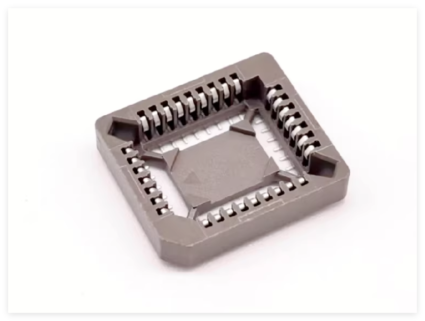

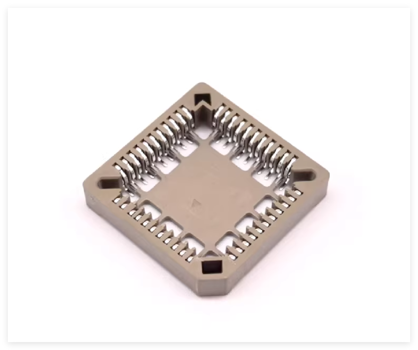

Ansix Tech Co Ltd
If you have any plans related to PEEK chip socket , you can contact us at any time. We will turn your ideas into reality, let you realize your dreams, and obtain large orders from the market. Our contact information is info@ansixtech.com. Or contact our CTO, mail: stephen@ansixtech.com
#www.ansixtech.com #ansixtech.com #PEEK chip socket #PEEK chip socket injection molding factory #Ansix injection mould #PEEK chip socket factory #PEEK chip socket injection molding company #PEEK chip socket injection mold companies #Ansix #Ansix moulds #Ansix china #Ansix tech china #Ansix tech company #Ansix facotry #Ansix Tech #Ansix molds #Ansix injection molding #Ansix mold factory #injection molding PEEK chip socket # Ansix mold factory #PEEK chip socket china #PEEK chip socket precision molds #injection factory #PEEK chip socket precision injection molding #L-shaped medical tumold injection molding factory #injection molding company #PEEK chip socket injection mold companies #PEEK chip socket factory #PEEK chip socket mold limited #Ansix mold china #Ansix companies #Ansix company China #PEEK chip socket facotry #Ansix Tech #Ansix Tech mould #PEEK chip socket injection moulding #injection moulding company #Ansix PEEK chip socket parts injection mold companies #PEEK chip socket #PEEK chip socket china #PEEK chip socket china factory #Ansix moulding companies #Ansix molding company #PEEK chip socket injection moulding facotry #Ansix Tech mold #PEEK chip socket precision mould #PEEK chip socket plastic injection molding #ansix plastic mold #Mold manufacturing #PEEK chip socket parts manufacturing #PEEK chip socket plastic parts factory #PEEK chip socket injection parts mold #PEEK chip socket PRECISION MANUFACTURING #PEEK chip socket precision #China mold #PEEK chip socket injection moulding china #PEEK chip socket mould china #china precision mold #mold in china #PEEK chip socket precision mold china #Precision molds #High-precision molds #PEEK chip socket #Injection molds #PEEK chip socket Factory #PEEK chip socket Company #Super Large Injection Mold Factory #Large Tonnage Injection Molding Factory #PEEK chip socket Company #PEEK chip socket Factory #2800T Injection Molding Factory #3000 Ton Injection Molding #4500 Ton Injection Molding Factory #Large Mold Injection Molding #Large Plastic Mold Injection Molding Factory #Large Injection Mold Manufacturer #Plastic Mold Factory #Injection Mold #Plastic Mold